Microsectioning, also known as Cross-sectioning or Metallographic Preparation, is the art of taking a two dimensional slice out of a sample to uncover an important feature.
This microsectioning or cross-sectioning technique can be used for a variety of applications, for example, revealing coating layer uniformity and thickness in plating finishes, or ascertaining the nature of the interface between the solder and Printed Circuit Board (PCB).
 The process of microsectioning is multi-stage and starts with the isolation of the area of interest from the rest of the assembly. This could involve delicately cutting an area around an electronic component from a PCB.
Once isolated, the component is then encapsulated into a potting medium (e.g., epoxy resin) within a mould and is left to cure.
On solidification, the mounted sample, or microsection, is retrieved from the mould and the sample face is gradually receded back using a series of abrasive material.
Once the features is revealed by this cross-sectioning, the microsection face is subjected to a number of polishing stages to generate a highly reflective finish that is then ready for optical and/or electron microscopy analysis to check such things as the plating thickness, coating thickness or failures in the solder joint.
 |
 |
 |
 |
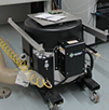
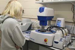
The key pieces of kit in the microsectioning process, namely the encapsulating materials, grinding wheel and automated polishing system. ITA Labs’ UK laboratory is extremely experienced at providing sample analysis test results, with a fast turnaround, at very competitive rates.
To discuss your potential requirements, call Tony in our microsectioning lab, on 01727 871326.

+44 (0)1727 871326
Our team of expert consultants and technologists at ITA Labs, utilising a state-of-the-art laboratory, can assist with all your product development and testing needs. With over 90 years of specialist knowledge in materials analysis and troubleshooting, we offer independent and impartial support. We cater to a variety of sectors, including electronics, fire testing, fire retardant and polymer product development, tinplate packaging, and surface coating technology. Our organisation is designed to respond swiftly to projects of any size.
Subscribe to our Mailing List
- ITA Labs, International Tin Association Ltd. Registered in England Number: 2994115 -
© 2026 ITA Labs - All rights reserved